In high school, you probably never learned about one of the most important types of materials: semiconductors. In my AP chemistry class, we divided elements into metals, nonmetals, and metalloids. That kind of classification might lead you to think that semiconductors are some kind of “weakly conducting” material–but semiconductors actually have a much more useful property.
Semiconductors are materials with a highly controllable electrical conductivity. Semiconductors have a small band gap which engineers can use to switch between conducting and nonconducting. This property makes semiconductors extremely useful for transistors in computers and other electronics.
While semiconductors have electrical conductivity between that of metals and insulators, their most important property is their small band gap. If electrons have a certain amount of energy, they can pass the bandgap and transition from nonconducting to conducting. I’ll talk about bandgap later in the article in more detail because band gap is the most unique property of semiconductors.
Outline
What Are Semiconductors?
All materials can be placed in one of three categories, depending on their electrical conductivity: conductors (metals), insulators, and semiconductors. (There are also superconductors, but that’s a different story).
Before modern physics, scientists categorized these materials based on their ability to conduct electricity. Conductivity is the inverse of resistivity, and resistivity measures how difficult it is to push electrons through a material.
Materials like metals, which easily conduct electricity, were deemed electrical conductors. Materials that did not conduct electricity were called insulators. Before the idea of band gaps, I imagine that scientists considered most semiconductors to be insulators. However, the term “semiconductor” did exist, and the first documentation of a semiconducting diode effect was in the 1800s, although semiconductors wouldn’t become widely useful until the invention of the transistor in 1947.
With band gaps, we have a quantum-mechanical basis for defining metals, semiconductors, and insulators. I’ll explain the band gap in the next section, but here is the band-gap definition of these materials

- Metals have an overlapping valence band and conduction band
- Semiconductors have a small gap between the valence band and conduction band, that electrons can potentially be crossed
- Insulators have a large gap between the valence band and conduction band and conduction band, which can’t be crossed by electrons
This band gap is what allows semiconductors to conduct electricity when energy is provided, so semiconductors can function as on/off switches. The band gap of most semiconductors is between 0.25 and 2.5 eV.
What Is a Band Gap?
Band diagrams can help us understand conductors, semiconductors, and insulators. There are many features of the band diagram that are important to semiconductors, but for this article, you only need to know the band gap.
The band diagram shows the possible energy states for an electron. For a single element and electron, there are some very specific energy levels that the electron can exist in. If the energy is energized it can hop between these states, and if there is enough energy it’s even possible for the electron to leave the atom completely.

As you have a piece of metal with a terrifyingly large number of atoms and electrons, these allowed energy states for each atom basically merge into a “band” of continually allowed states. This is called the valence band.
Beyond the valence band is the conduction band. The conduction band is the collection of energy states where the electrons have enough energy to leave the atom that they’re bound to.
The band gap is the distance between these valence bands and conduction bands. The difference between metals, insulators, and semiconductors is the size of the band gap.
In other words, the band gap is the minimum energy required for an electron to leave the atom and start conducting.
Metals have no band gap. In other words, the conduction band and valence band overlap, so an atom is not bound to any particular atom. If it has enough energy to leave, it just leaves.
Semiconductors have a small band gap. This means that if the electrons don’t have enough energy to fully jump across the band gap, the semiconductor does not conduct at all. If there is enough energy to pass this barrier, the material conducts. Semiconductors are super useful because they can act as switches, either passing 0% or 100% of the current.
Insulators have a large band gap. The distinction between insulator and semiconductor is a bit nebulous–it’s not like scientists have a simple value and if the band gap is larger than that value, it’s an insulator. These terms are practical–anything which is considered an insulator has a band gap that is too large to cross in a realistic scenario. Trying to pass too much current through many insulators will destroy the material before electrons have enough energy to jump across the band gap.
| Type of Material | Material | Band Gap |
| Semiconductor | Si GaN | 1.12 eV 3.44 eV |
| Insulator | diamond PE (polyethylene) | 5.47 eV 8.8 eV |
Examples of Semiconducting Materials
Many materials can be semiconducting. Pure elements like Si and Ge can be semiconductors, as well as compounds, oxides and organic-based materials.
A common technique to control the conductivity of semiconductors is doping. Since semiconductors are usually used for their electric properties, they are also made as single crystals so grain boundaries don’t scatter electrons.
Here is a list of some common semiconductors, and their band gaps:
| Semiconductor | Band Gap Energy |
| Si | 1.12 eV |
| Ge | 0.67 eV |
| GaN | 3.44 eV |
| GaP | 2.26 eV |
| GaAs | 1.43 eV |
| PbS | 0.37 eV |
| Cu2S | 1.2 eV |
| Cu2O | 2.17 eV |
| β-SiC | 2.36 eV |
| CdS | 1.74 eV |
| CdTe | 1.49 eV |
How Do Semiconductors Conduct Electricity?
Conductivity measures the amount of electrical current a material can carry. It can also be called “specific conductance” and is the inverse of resistivity.
- Conductivity is inversely proportional to resistivity! (high conductivity = low resistance)
- Units: Resistivity, ρ (Ω·m); Conductivity, σ (1/(Ω·m) =S/m)
In conductors, the charge carrier is just electrons. But in semiconductors we have both electrons and holes. Electrons have a charge of -1 and holes have a charge of +1.

With this model of electrons and holes, conductivity happens when electrons and holes move in the opposite direction.

Conductivity is given by the following equation.

n and p are the carrier density–in other words, how many electrons and holes exist per cross-sectional area. n is for negatively charged carriers (electrons) and p is for positively charged carriers (holes). This can be changed by doping. If the semiconductor is doped, either n or p will be much larger than the other, so the conductivity equation can be approximated as  or
or  . N-type semiconductors tend to be more common because the mobility of electrons is usually higher than the mobility of holes. For example, the mobility of electrons is 3 times higher than holes in intrinsic silicon at room temperature.
q is the electric charge of each carrier–for electrons and holes, this is 1.
 is the mobility, which is how quickly the electron or hole can move through the material.
Conductivity in semiconductors strongly depends on:
- temperature (more energy to bridge the band gap)
- illumination (more energy to bridge the band gap)
- tiny amounts of impurity atoms (dopants)
For semiconductors to conduct, charger carriers need enough energy to bridge the band gap.

If free electrons and holes can be created, they will respond to an electric field, conducting electricity.
However, you can’t take the presence of free electrons and holes for granted. These can only exist because of external energy–usually thermal or light.
Here, you can see how important temperature is to semiconductor conductivity.

Semiconductor conductivity increases exponentially with temperature because more electrons reach the conduction band.
Another way to think of this is that some covalent bonds break with increasing temperature. These free electrons can now participate in electrical conduction.
Using  , increasing temperature dramatically increase
  and
and  . decreases slightly, but it is negligible compared to the increase in charge carriers.

Types of Semiconductors
Semiconductors can be divided into two groups: intrinsic semiconductors and extrinsic semiconductors. Extrinsic semiconductors are doped, which means some small amounts of impurities are added to improve conductivity. Intrinsic semiconductors are not doped–or more precisely, they have the same number of electrons and holes.

Intrinsic semiconductors conduct because of migration of electrons and holes. Since increasing the temperature gives electrons enough thermal energy to pass the band gap, the number of electrons and holes increases with temperature. However, the number of charge carriers is still much lower in intrinsic semiconductors than extrinsic (doped) semiconductors.
To make extrinsic semiconductors, engineers dope the material with a different-valence element. I’ll use silicon as the general example for this.
Silicon is a group IV semiconductor: it has 4 electrons in its valence shell. By adding small amounts of gallium (a group III element with 3 electrons in its valence shell), holes would be created. Each atom of boron would create one additional hole. Since B binds an electron, it is an acceptor atom. This kind of doping results in an P-type semiconductor.

If arsenic (a group VI element with 5 electrons in its valence shell) was added to Si, there would be extra unbound electrons. Each atom of arsenic would contribute an additional n charge carrier. Since As adds a free electron, it is a donor atom. This kind of doping results in a N-type semiconductor.

If arsenic and gallium were added together, the semiconductor would still have the same number of holes and free electrons, so it would be intrinsic. GaAs is an intrinsic semiconductor, although only if it has exactly the same amount of Ga and As. GaAs is a semiconductor that can be self-doped; for example, by having slightly more Ga than As. This kind of doping results in an N-type semiconductor.
Here is a summary table of the difference between N- and P-type semiconductors.
| P-type Semiconductors | N-type Semiconductors |
| Extrinsic semiconductors | Extrinsic semiconductors |
| Holes are major current carriers | Electrons are major current carriers |
| Doping is achieved by adding atoms with fewer (than host atoms) valence electrons = acceptor atoms | Doping is achieved by adding atoms with more (than host atoms) valence electrons = donor atoms |
| Fermi level lies between the valence band and the acceptor (hole) energy level | Fermi level lies between the donor (electron) energy level and the conduction band |
| Group III atoms are added to the lattice of group IV atoms | Group V atoms are added to the lattice of group IV atoms |
| Examples of acceptors: B, Ga, In, Al | Examples of donors: P, As, Sb, Bi |
Using the band gap diagram, you can think of doping as adding possible energy states. N-type doping adds new levels for electrons below the conduction band, and P-type doping adds new energy levels above the valence band.

These new energy levels shift the effective Fermi level, making conduction much easier.
Manufacturing Techniques of Semiconductor
Semiconductors are usually single crystals. Actually, silicon wafers are arguably the most-perfect arrangement of atoms in the universe. Billions of dollars are spent keeping them as defect-free as possible, since every defect affects semiconducting properties.
To make single crystals, semiconductors can be cast in the Czochralski method.
In this method, the liquid material sits in a crucible very close to the melting temperature. A crystal nucleus seeds crystal growth, and new atoms grow from there. As the nucleus is pulled out, more atoms stick until the entire liquid has solidified into a single crystal.

This single crystal log is then cut into wafters to use in integrated circuits for computers, TVs, phones, and other devices, or in solar cells. Monocrystalline silicon made by this method is called Czochralski silicon, or Cz-Si.
Single crystal semiconductors can also be deposited as a film by epitaxial growth. Epitaxial growth is when the semiconductor is grown directly on a substrate. It is often grown by vapor-phase epitaxy, a type of chemical vapor deposition (CVD).
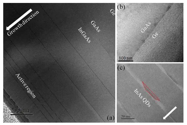
InAs QDs monolithically grown on Ge substrate” publication
Applications of Semiconductors
Semiconductors are used in power devices, optical sensors, light emitters (LED), solid-state lasers, RF applications, diode (p-n junction), MOSFETs, photovoltaics, and more.
I want to focus on 3 main devices that use semiconductors and are useful to make other things: diodes, transistors, and photovoltaics.
Diodes
Diodes are devices that only allow current to flow in one direction. They work because of a P-N junction. A P-N junction means that you connect a P-type semiconductor to an N-type semiconductor.

Since the N-type semiconductor has excess electrons and the P-type semiconductor has excess holes, there is a tendency for electrons to migrate over the junction. However, this depletion region will have an electrical potential, repulsing further electron exchange.
If an external electric potential (like voltage from a battery) is applied to push the electrons from the N-type to the P-type, the depletion region can be overcome and electricity will flow. We call this a forward bias.
If the external electric potential tries to pull electrons and holes away from each other, the electrons will build up a large negative charge that will counteract the external potential, preventing electric flow in that direction. We call this a reverse bias.
Diodes can be used for many applications such as radio demodulation, power conversion, logic gates, reverse voltage protection, light-emission, and more.
Light-emitting diodes (LEDs) are a special type of diode that takes advantage of recombination. Recombination is when an electron and hole come together. Recombination emits energy because the electron drops from the conduction band to the valence band. Since the energy emitted is light, the color of the light relates to its energy. The energy corresponds to the band gap size, so the band gap determines the color of energy emitted.
In most diodes, the energy emitted is in the infrared range, so we can’t see it. LEDs are made of semiconductors with a band gap such that the energy emitted corresponds to the visible spectrum.
Transistor
Transistors are basically switches. They are used extensively in electronics as a way to store 0 and 1.
If you understood how diodes work, a transistor is essentially 2 diodes back-to-back. Here is a common type of transistor called a MOSFET (Metal Oxide Silicon Field Effect Transistor)

You have an N-type, P-type, N-type arrangement of semiconductors. As with diodes, there is some recombination at the P-N junctions, but this creates a depletion layer that repels further charge transfer. However, if a voltage is applied, the depletion layer can be overcome and it will conduct electricity. Remove the voltage, and conduction stops.
Transistors are very powerful because they are small, can change states rapidly, and have no moving parts. They can be used as billions of on/off switches in computers or other electronics.
Photovoltaics
Photovoltaics, or solar cells, also work by a P-N junction. At the junction, free electrons fill the holes. However, the electrons and holes can be separated by hitting them with energy equal to–you guessed it–the band gap.
Solar cells generate electricity by sweeping away these free electrons as they are generated, and preventing them from recombining again.
That’s why the top N-layer is thin–the light has to pass through this layer to hit the neutral junction between the N-layer and P-layer. Electrons which are split from their holes in this layer will migrate to the top and follow the conducting wire that lets them return to the P-layer while work is extracted.

Final Thoughts
Semiconductors are materials that have a variable conductivity depending on the energy that electrons have to pass the band gap. One of the most common kinds of semiconductor is Si, with a band gap of 1.1 eV.
They are the backbone of computers. Modern technology would not be possible without transistors and diodes.
References and Further Reading
If you are interested in electronic properties of materials, you may be interested in our article about why metals conduct electricity.
If you like functional materials, you can find our main article on magnetism here.
This is the paper where we got the image of epitaxial growth:
Wen-Qi Wei, Jian-Huan Wang, Yue Gong, Jin-An Shi, Lin Gu, Hong-Xing Xu, Ting Wang, and Jian-Jun Zhang, C/L-band emission of InAs QDs monolithically grown on Ge substrate, Opt. Mater. Express 7, 2955-2961 (2017)