If there is a tool that is most-used by materials scientists, that tool is the Scanning Electron Microscope (SEM). The SEM allows scientists to observe materials at length scales that are too small for visible light.
The Scanning Electron Microscope (SEM) is one of the most versatile characterization techniques for materials. SEM can determine microstructure (BSE), morphology (SE), and elemental composition (EDS) of electrically conductive samples.
SEMs can have a resolution as low as 1 nm (over 100,000x magnification), although the resolution is not as good as TEM (Transmission Electron Microscopy) which can even detect columns of atoms.
SEM can also be used for non-conductive samples, but those samples will need an electrically conductive coating. This makes SEM a powerful tool for biologists, but sample preparation is annoying for them.
As a metallurgist, SEM is the most convenient–and one of the most-powerful–tools for my samples. In this article, I’ll explain everything you need to know about SEM, including specific detectors such as backscatter electron (BSE), secondary electron (SE), Energy Dispersive X-Ray Spectroscopy (EDS), and Electron Backscatter Diffraction (EBSD).
Outline
How Does SEM Work?
Scanning Electron Microscopes work pretty much the same way that optical microscopes do. In an optical microscope, light is emitted onto a sample. That light reflects from the sample and is captured, focused, and magnified by lenses.
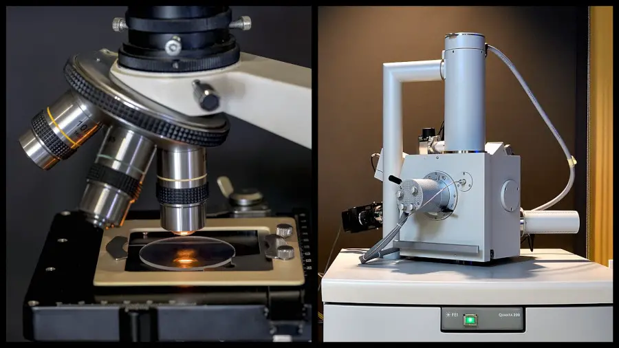
Similarly, SEMs have an electron gun which shoots electrons at the sample. The process isn’t exactly reflection (I’ll explain more when I talk about SE and BSE) but the electron gun does cause electrons to emit from the sample. These electrons are captured, focused, and magnified by magnetic lenses, and then detected by the SEM. The SEM converts the detected electrons into a digital image that you can see on your computer screen.
That’s the basic principle, but let’s dive a bit deeper into how the SEM actually works. Scanning Electron Microscopes have an electron gun, condenser and objective lenses, condenser and objective apertures, scan coils, and electron detectors. All of this also needs to be in a vacuum chamber so the electrons are not disturbed by gas molecules. Electrons are not as simple to manipulate as photons!

Let’s start with the electron gun. The gun needs a voltage to accelerate electrons toward the sample, but first those electrons need to be created. There are three general ways to produce these electrons: Thermionic Emission, Field Emission, and Schottky Emission.
Thermionic Emission uses a filament (usually tungsten, for obvious reasons) and heats it up. The increase in temperature causes electrons to be released. Similar to the photoelectric effect, heating a cathode (like metal) in a vacuum will cause electrons to gain enough energy to leave the cathode. This is one way to create an electron beam.
The second way to generate electrons is by Field Emission, which comes from quantum mechanical effects. Instead of increasing temperature, a very high voltage is applied to the cathode. This creates an electron beam. Field Emission electron guns can provide a better resolution than thermionic emission electron guns.
The third type of electron beam is generated by Schottky Emission, which is also called a thermal field emission gun. This kind of emission comes from high temperature AND high voltage. The beam has a larger spread, but also larger probe currents.
Here is a bar graph showing the relative pros and cons of the three kinds of electron guns.

After the electron source, there is an accelerating voltage. This creates an electric field which propels the electrons into a beam which shoots through the microscope.
Not only is a vacuum required to create electron emission, vacuum is essential to avoid ionized gases from the high-energy electrons.
A scanning electron microscope uses a magnetic lens to focus the electrons. The condenser lens focuses the electron beam as it leaves the gun. The condenser aperture is basically a hole that only allows part of the beam (just like a light aperture in a camera or optical microscope). The condenser lens and aperture ensure that the electron beam which hits the sample is focused and there are no stray electrons which might confuse the signal. When SEM detectors pick up scattered electrons, the original direction and velocity is guaranteed.
The scan coils direct the electron beam in a raster pattern so that it is possible to view an area of the sample larger than the electron beam size.
The objective lens and aperture provide the final focus between the electron beam and the sample.
After the electron beam leaves the objective aperture, it falls onto the sample. The sample must be electrically conductive to return a signal that can be detected.
There are many types of signals that are produced when electrons interact with the sample.

- Electrons from the electron beam can collide inelastically with atoms. Since energy is lost from the electron, that energy needs to go somewhere else. Usually, a lower-energy electron from the atom is also ejected. These electrons are called secondary electrons (SE).
- If the electrons from the electron beam collide elastically with an atom, the electron will change trajectory. These electrons are called backscattered electrons (BSE).
- Electron backscatter diffraction (EBSD) is a further technique that can take advantage of backscattered electrons. Since these electrons are produced deeper inside the sample, they may exit at the Bragg condition, which provides information on the spacing between atoms.
- In rare cases, an electron from the electron beam can knock out a core electron from an atom. This will cause a higher-level electron to drop down, releasing a quantum of energy. Although this energy packet is usually a photon, sometimes it may be an electron. If it is an electron, the electron is called an Auger Electron. However, auger electrons are not usually detected in SEM.
- Additionally, electron collisions with atoms can release X-ray radiation. This radiation is related to the distance between atomic suborbitals, and is unique for every element. These X-rays are called Characteristic X-Rays. Continuum and Fluorescent X-rays also exist, but these are not usually useful in SEM. Energy Dispersive X-Ray Diffraction (EDS) is an SEM technique that detects characteristic X-rays.
As you can see below, different types of electrons and X-ray signals come from different depths of the sample. Depending on the beam accelerating voltage, spot size, and aperture; as well as the material itself, the electron beam may penetrate different depths into the sample.
This image also shows that as the beam penetrates the sample, it widens. Thus, resolution is lost. That is why signals from secondary electrons have higher resolution than from backscattered electrons. I’ll discuss SE and BSE techniques more in the next section.

Applications of SEM
SEM can be applied to materials that conduct electricity. If they don’t, you need to cover your sample with a thin metallic film (for example to examine biological samples like insects). Some SEMs can operate under low-vacuum mode to examine non-conductive samples. Samples will always need to be dehydrated, however.
SEM is an extremely versatile tool which is relatively easy to learn and to prepare samples for, compared to something like TEM or atom probe tomography. SEM is used in
- Materials science, for general research, quality control, and failure analysis purposes. It can detect chemical composition, morphology, topography, and microstructure. SEM is used to inspect semiconductors and microchip assemblies.
- Forensic Science for things like currency examination, handwriting analysis, art restoration, crime scene evidence, and more.
- Biology, for insect parts, animal tissue, or even bacteria/virus imaging.
Here are some ways that specific SEM techniques can be used in different applications:
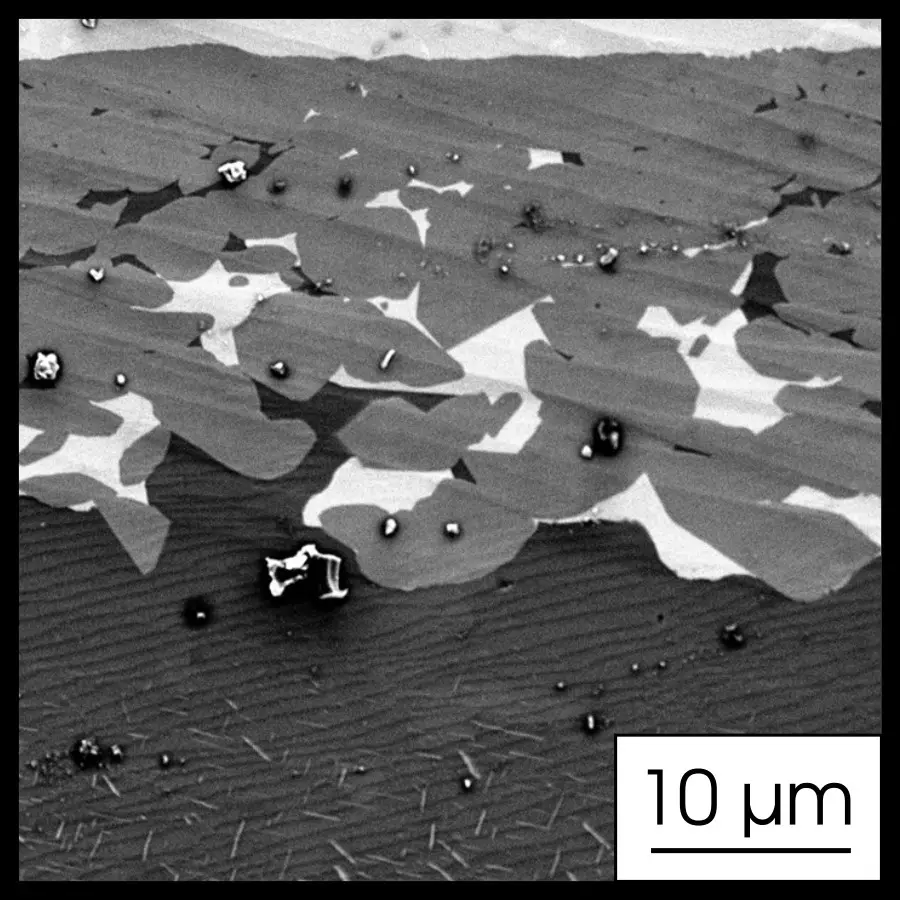
BSE (Backscattered Electrons) is great for metals. It highlights microstructure and shows how different phases are arranged. BSEs come from a broad interaction volume because they arise from elastic collisions between the electron bean and atoms. The electrons from the beam bounce away with the same energy but a different direction. Since larger atoms are more likely to cause the electrons to bounce, better signal comes from heavier atoms. In fact, the number of BSEs that reach the detector is proportional to the atomic weight of the atoms. Thus, BSE gives a visual representation of the average atomic weight of an area, and can spot non-metallic inclusions. Additionally, BSE images can provide information on crystallography, topography, and magnetic field.
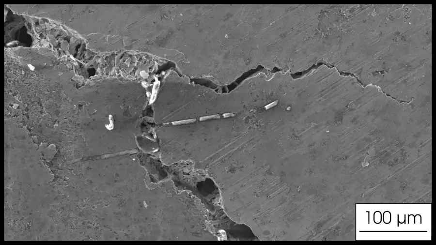
SE (Secondary Electrons) is great for analyzing the surface of a sample. These electrons come from the inelastic interaction of the main electron beam and atoms, so SEs come from the sample surface and have lower energy than BSEs. If you want to use a colorless optical microscope with higher resolution, SE analysis is your tool. It shows topography. As a metallurgist, SE is useful to analyze cross sections after tensile tests to determine whether the material is brittle or ductile, crack observation, interface observations, and corrosion. Since SE has higher resolution than BSE, a well-etched sample may look better in SE than BSE.
EDS (Energy Dispersive X-Ray Spectroscopy), which may also be called EDX or EDXS, is used to determine/analyze chemical composition of different materials, layers, etc. You can detect what elements are present in the examined sample, and even create maps to figure out the composition of precipitates. If I were handed a mystery metal and had to figure out what it’s made of, EDS would be my first tool.

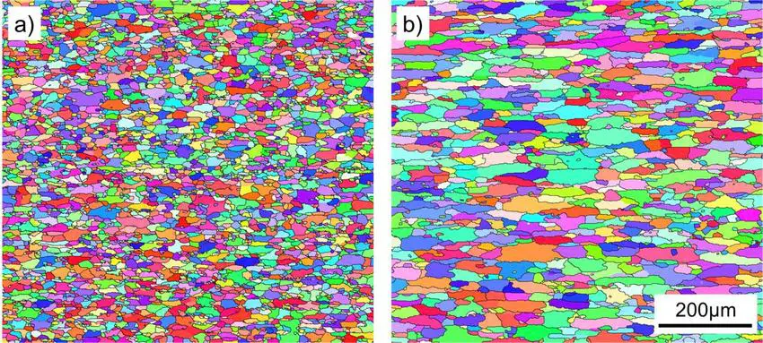
EBSD (Electron Backscatter Diffraction): to determine local texture and grain orientation, which might be present after something like cold rolling. It can distinguish between low and high angle grain boundaries, or help determine which grain will fail in a sample because of the critical resolved shear stress.
Limitations of SEM
The most direct limitation of SEM, actually, is no longer its price tag. New SEMs can cost around $1 million (which is not THAT much compared to some other equipment), but SEM technology is common enough now that it’s possible to buy cheaper or previously-used SEMs for low six-figures. Actually, some used SEMs can cost only $15,000! Most research universities and large companies have several scanning electron microscopes.
The main limitation of SEM is the sample preparation. For bulk metal samples, SEM is easy. You need to polish and etch the sample, embed it in resin so it doesn’t move in the microscope, and apply conductive strips so the metal completes a circuit with the SEM stage. Metal samples usually won’t be damaged by vacuum or the electron beam.
Non-metal samples are trickier to use in SEM. They need to be conductive, which can be achieved by applying a thin film of metal such as gold. The samples also need to be dehydrated (especially if it’s a biological sample) because water will boil in vacuum. In some cases it may be possible to use the SEM in low-vacuum mode, but with some drawbacks.
In many materials, the electron beam may also degrade the sample. The beam would have to have lower energy to prolong the sample lifetime, in this case.
SEM cannot penetrate very deeply into the material surface–other techniques are better for this information.
SEMs usually have small chambers, which makes it difficult to fit large samples inside. While SEM itself is usually non-destructive, it may be necessary to cut a small piece from a work of art if you wanted to view the artwork in SEM.

Final Thoughts
SEM is one of the most versatile characterization techniques available. For many materials (especially metals), it is cheap, easy-to-use, and fast. SEM is usually non-destructive, which is another bonus.
SEM can view secondary electrons (SE) which come from inelastic scattering and give surface-level information, or backscattered electrons (BSE) which come from elastic scattering and provide information about atomic weight.
Here is a summary table about the 4 main techniques in SEM: backscattered electrons, secondary electrons, energy-dispersive x-ray spectroscopy, and electron backscatter diffraction.
| Detector | Backscattered Electrons (BSE) | Secondary Electrons (SE) | Energy-Dispersive X-Ray Spectroscopy (EDS) | Electron Backscatter Diffraction (EBSD) |
| What is detected? | BSEs (elastic electron-atom interaction) | SEs (inelastic electron-atom interaction). SEs have lower energy than BSEs | Characteristic X-ray radiation (specific for each element) | BSEs which satisfy Bragg condition |
| What kind of contrast is achieved? | Mass (Z number) | Topographic (“3D” effect) | Chemical | Grain orientation |
| What can we learn about a material? | Phase distribution, layer thickness, microstructure homogeneity, presence of non-metallic inclusions | Surface condition (traces of corrosion, oxidation, fatigue), morphology, voids, cracks, cross-sections (ductile, brittle) | Chemical composition of whole materials, layers, homogeneity | Grain orientation, misorientation angle, local texture |
| Relative resolution | Medium | Highest | Lowest | Medium |
| Acquisition time | Almost none (<1s) | Almost none (<1s) | Varies (point, line-scan, mapping) can take several minutes | From a few minutes up to a few hours, depending on a grain size |
| Required sample preparation | polishing (sometimes etching) | polishing or none (when observing cross sections) | polishing | polishing |
| Typical limitations | Lower resolution than SE | Although SE is suitable for “3D” images, the examined surface shouldn’t be too rough | Difficulties in assessing light elements content like C, N, O | Grain size (not suitable for nanoscale grains) |
References and Further Reading
If you are an advanced high school student who found this article because you wanted to learn about SEM, you may also be interested in materials science! Here is our article that will help you decide if materials science is the right major for you.
If you’re interested in learning more about SEM, check out Scanning Electron Microscope A To Z from a company that makes these microscopes.
Here you’ll find a great resource on EBSD by Oxford Instruments.