SEM is the abbreviation for Scanning Electron Microscope or Scanning Electron Microscopy.
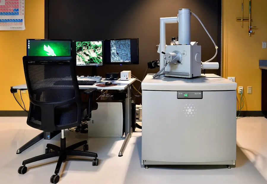
Scanning Electron Microscopy (SEM) is any technique that involves the instrument which is called a Scanning Electron Microscope (SEM).
SEM is an electron microscope. That means that it shoots electrons at a sample and detects those electrons, the same way your eyes detect photons.
SEM is primarily used on conductive samples like metals. It can also be used on biological samples, but these need to be covered with a conductive coating.
SEM offers better resolution than optical microscopy (OM) but worse resolution than transmission electron microscopy (TEM). However, SEM is less convenient than OM, but more convenient than TEM.

SEM primarily used to perform one of three types of imaging: secondary electron (SE), backscatter electron (BSE), or energy dispersive X-ray spectroscopy (EDS).
This article is just a definition. If you would like to learn more about SEM and these techniques, check out my full article here.
Related Terms:
SE (Secondary Electron)
BSE (Backscatter Electron)
EDS, also called EDX or EDXS (Energy Dispersive X-Ray Spectroscopy)
OM (Optical Microscope)
TEM (Transmission Electron Microscope)